- 您现在的位置:买卖IC网 > Sheet目录319 > COP8SG-EPU (National Semiconductor)BOARD PROTOTYPE/TARGET COP8
�� �
�
�WATCHDOG�
�The� device� contains� a� WATCHDOG� and� clock� monitor.� The�
�WATCHDOG� is� designed� to� detect� the� user� program� getting�
�stuck� in� infinite� loops� resulting� in� loss� of� program� control� or�
�“runaway”� programs.� The� Clock� Monitor� is� used� to� detect� the�
�absence� of� a� clock� or� a� very� slow� clock� below� a� specified�
�rate� on� the� CKI� pin.�
�The� WATCHDOG� consists� of� two� independent� logic� blocks:�
�WD� UPPER� and� WD� LOWER.� WD� UPPER� establishes� the�
�upper� limit� on� the� service� window� and� WD� LOWER� defines�
�the� lower� limit� of� the� service� window.�
�Servicing� the� WATCHDOG� consists� of� writing� a� specific�
�value� to� a� WATCHDOG� Service� Register� named� WDSVR�
�which� is� memory� mapped� in� the� RAM.� This� value� is� com-�
�posed� of� three� fields,� consisting� of� a� 2-bit� Window� Select,� a�
�5-bit� Key� Data� field,� and� the� 1-bit� Clock� Monitor� Select� field.�
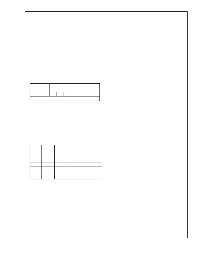
�Table� 6� shows� the� WDSVR� register.�
�TABLE� 6.� WATCHDOG� Service� Register� (WDSVR)�
�occur� after� coming� out� of� reset,� if� the� instruction� cycle� clock�
�frequency� has� not� reached� a� minimum� specified� value,� in-�
�cluding� the� case� where� the� oscillator� fails� to� start.�
�The� WDSVR� register� can� be� written� to� only� once� after� reset�
�and� the� key� data� (bits� 5� through� 1� of� the� WDSVR� Register)�
�must� match� to� be� a� valid� write.� This� write� to� the� WDSVR� reg-�
�ister� involves� two� irrevocable� choices:� (i)� the� selection� of� the�
�WATCHDOG� service� window� (ii)� enabling� or� disabling� of� the�
�Clock� Monitor.� Hence,� the� first� write� to� WDSVR� Register� in-�
�volves� selecting� or� deselecting� the� Clock� Monitor,� select� the�
�WATCHDOG� service� window� and� match� the� WATCHDOG�
�key� data.� Subsequent� writes� to� the� WDSVR� register� will�
�compare� the� value� being� written� by� the� user� to� the� WATCH-�
�DOG� service� window� value� and� the� key� data� (bits� 7� through�
�1)� in� the� WDSVR� Register.� Table� 8� shows� the� sequence� of�
�events� that� can� occur.�
�The� user� must� service� the� WATCHDOG� at� least� once� before�
�the� upper� limit� of� the� service� window� expires.� The� WATCH-�
�DOG� may� not� be� serviced� more� than� once� in� every� lower�
�limit� of� the� service� window.� The� user� may� service� the�
�WATCHDOG� as� many� times� as� wished� in� the� time� period� be-�
�Window�
�Select�
�Key� Data�
�Clock�
�Monitor�
�tween� the� lower� and� upper� limits� of� the� service� window.� The�
�first� write� to� the� WDSVR� Register� is� also� counted� as� a�
�X�
�X�
�0�
�1�
�1�
�0�
�0�
�Y�
�WATCHDOG� service.�
�7� 6� 5� 4� 3� 2� 1� 0�
�The� lower� limit� of� the� service� window� is� fixed� at� 2048� instruc-�
�tion� cycles.� Bits� 7� and� 6� of� the� WDSVR� register� allow� the�
�user� to� pick� an� upper� limit� of� the� service� window.�
�Table� 7� shows� the� four� possible� combinations� of� lower� and�
�upper� limits� for� the� WATCHDOG� service� window.� This� flex-�
�ibility� in� choosing� the� WATCHDOG� service� window� prevents�
�any� undue� burden� on� the� user� software.�
�Bits� 5,� 4,� 3,� 2� and� 1� of� the� WDSVR� register� represent� the�
�5-bit� Key� Data� field.� The� key� data� is� fixed� at� 01100.� Bit� 0� of�
�the� WDSVR� Register� is� the� Clock� Monitor� Select� bit.�
�TABLE� 7.� WATCHDOG� Service� Window� Select�
�The� WATCHDOG� has� an� output� pin� associated� with� it.� This�
�is� the� WDOUT� pin,� on� pin� 1� of� the� port� G.� WDOUT� is� active�
�low.� The� WDOUT� pin� is� in� the� high� impedance� state� in� the� in-�
�active� state.� Upon� triggering� the� WATCHDOG,� the� logic� will�
�pull� the� WDOUT� (G1)� pin� low� for� an� additional� 16� t� c� –32� t� c�
�cycles� after� the� signal� level� on� WDOUT� pin� goes� below� the�
�lower� Schmitt� trigger� threshold.� After� this� delay,� the� device�
�will� stop� forcing� the� WDOUT� output� low.�
�The� WATCHDOG� service� window� will� restart� when� the� WD-�
�OUT� pin� goes� high.� It� is� recommended� that� the� user� tie� the�
�WDOUT� pin� back� to� V� CC� through� a� resistor� in� order� to� pull�
�WDOUT� high.�
�A� WATCHDOG� service� while� the� WDOUT� signal� is� active� will�
�be� ignored.� The� state� of� the� WDOUT� pin� is� not� guaranteed�
�on� reset,� but� if� it� powers� up� low� then� the� WATCHDOG� will�
�WDSVR� WDSVR�
�Clock�
�Service� Window�
�time� out� and� WDOUT� will� enter� high� impedance� state.�
�Bit� 7�
�0�
�0�
�1�
�1�
�x�
�x�
�Bit� 6�
�0�
�1�
�0�
�1�
�x�
�x�
�Monitor�
�x�
�x�
�x�
�x�
�0�
�1�
�(Lower-Upper� Limits)�
�2048–8k� t� C� Cycles�
�2048–16k� t� C� Cycles�
�2048–32k� t� C� Cycles�
�2048–64k� t� C� Cycles�
�Clock� Monitor� Disabled�
�Clock� Monitor� Enabled�
�The� Clock� Monitor� forces� the� G1� pin� low� upon� detecting� a�
�clock� frequency� error.� The� Clock� Monitor� error� will� continue�
�until� the� clock� frequency� has� reached� the� minimum� specified�
�value,� after� which� the� G1� output� will� enter� the� high� imped-�
�ance� TRI-STATE� mode� following� 16� t� c� –32� t� c� clock� cycles.�
�The� Clock� Monitor� generates� a� continual� Clock� Monitor� error�
�if� the� oscillator� fails� to� start,� or� fails� to� reach� the� minimum�
�specified� frequency.� The� specification� for� the� Clock� Monitor�
�is� as� follows:�
�Clock� Monitor�
�The� Clock� Monitor� aboard� the� device� can� be� selected� or� de-�
�selected� under� program� control.� The� Clock� Monitor� is� guar-�
�anteed� not� to� reject� the� clock� if� the� instruction� cycle� clock� (1/�
�t� c� )� is� greater� or� equal� to� 10� kHz.� This� equates� to� a� clock� input�
�rate� on� CKI� of� greater� or� equal� to� 100� kHz.�
�1/t� c� >� 10� kHz� —� No� clock� rejection.�
�1/t� c� <� 10� Hz� —� Guaranteed� clock� rejection.�
�WATCHDOG� AND� CLOCK� MONITOR� SUMMARY�
�The� following� salient� points� regarding� the� WATCHDOG� and�
�CLOCK� MONITOR� should� be� noted:�
�?� Both� the� WATCHDOG� and� CLOCK� MONITOR� detector�
�WATCHDOG� Operation�
�The� WATCHDOG� and� Clock� Monitor� are� disabled� during� re-�
�set.� The� device� comes� out� of� reset� with� the� WATCHDOG�
�armed,� the� WATCHDOG� Window� Select� bits� (bits� 6,� 7� of� the�
�WDSVR� Register)� set,� and� the� Clock� Monitor� bit� (bit� 0� of� the�
�WDSVR� Register)� enabled.� Thus,� a� Clock� Monitor� error� will�
�www.national.com�
�38�
�?�
�?�
�circuits� are� inhibited� during� RESET.�
�Following� RESET,� the� WATCHDOG� and� CLOCK� MONI-�
�TOR� are� both� enabled,� with� the� WATCHDOG� having� he�
�maximum� service� window� selected.�
�The� WATCHDOG� service� window� and� CLOCK� MONI-�
�TOR� enable/disable� option� can� only� be� changed� once,�
�during� the� initial� WATCHDOG� service� following� RESET.�
�发布紧急采购,3分钟左右您将得到回复。
相关PDF资料
CORE1553-DEV-KIT
KIT DEVELOPMENT FOR IP CORE1553
CP131-AG
LNR PWR SUP 5V 8A, +/-12V 1.7A
CPC1590P
MOSFET GATE DVR ISO 8-FLATPACK
CPC5002G
ISOLAT DGTL 3.75KVRMS 2CH 8-DIP
CPCI-D-3U-300C
PWR SUPLY DC/DC CPCI 300W 3UX8HP
CPD250-4530G
PWR SUP 250W 3.3/5/12/-12V QUAD
CS4161YN8
IC DRIVER H-BRDG DUAL 85MA 8DIP
CS5461A-ISZ
IC ENERGY METERING 1PHASE 24SSOP
相关代理商/技术参数
COP8SGR728M7
功能描述:8位微控制器 -MCU RoHS:否 制造商:Silicon Labs 核心:8051 处理器系列:C8051F39x 数据总线宽度:8 bit 最大时钟频率:50 MHz 程序存储器大小:16 KB 数据 RAM 大小:1 KB 片上 ADC:Yes 工作电源电压:1.8 V to 3.6 V 工作温度范围:- 40 C to + 105 C 封装 / 箱体:QFN-20 安装风格:SMD/SMT
COP8SGR728M7/NOPB
功能描述:8位微控制器 -MCU RoHS:否 制造商:Silicon Labs 核心:8051 处理器系列:C8051F39x 数据总线宽度:8 bit 最大时钟频率:50 MHz 程序存储器大小:16 KB 数据 RAM 大小:1 KB 片上 ADC:Yes 工作电源电压:1.8 V to 3.6 V 工作温度范围:- 40 C to + 105 C 封装 / 箱体:QFN-20 安装风格:SMD/SMT
COP8SGR728M8
功能描述:8位微控制器 -MCU RoHS:否 制造商:Silicon Labs 核心:8051 处理器系列:C8051F39x 数据总线宽度:8 bit 最大时钟频率:50 MHz 程序存储器大小:16 KB 数据 RAM 大小:1 KB 片上 ADC:Yes 工作电源电压:1.8 V to 3.6 V 工作温度范围:- 40 C to + 105 C 封装 / 箱体:QFN-20 安装风格:SMD/SMT
COP8SGR728M8/NOPB
功能描述:8位微控制器 -MCU RoHS:否 制造商:Silicon Labs 核心:8051 处理器系列:C8051F39x 数据总线宽度:8 bit 最大时钟频率:50 MHz 程序存储器大小:16 KB 数据 RAM 大小:1 KB 片上 ADC:Yes 工作电源电压:1.8 V to 3.6 V 工作温度范围:- 40 C to + 105 C 封装 / 箱体:QFN-20 安装风格:SMD/SMT
COP8SGR728N8
功能描述:8位微控制器 -MCU RoHS:否 制造商:Silicon Labs 核心:8051 处理器系列:C8051F39x 数据总线宽度:8 bit 最大时钟频率:50 MHz 程序存储器大小:16 KB 数据 RAM 大小:1 KB 片上 ADC:Yes 工作电源电压:1.8 V to 3.6 V 工作温度范围:- 40 C to + 105 C 封装 / 箱体:QFN-20 安装风格:SMD/SMT
COP8SGR728N8/NOPB
功能描述:8位微控制器 -MCU RoHS:否 制造商:Silicon Labs 核心:8051 处理器系列:C8051F39x 数据总线宽度:8 bit 最大时钟频率:50 MHz 程序存储器大小:16 KB 数据 RAM 大小:1 KB 片上 ADC:Yes 工作电源电压:1.8 V to 3.6 V 工作温度范围:- 40 C to + 105 C 封装 / 箱体:QFN-20 安装风格:SMD/SMT
COP8SGR740N8
功能描述:IC MCU 8BIT CMOS OTP 40DIP RoHS:否 类别:集成电路 (IC) >> 嵌入式 - 微控制器, 系列:COP8™ 8SG 其它有关文件:STM32F101T8 View All Specifications 特色产品:STM32 32-bit Cortex MCUs 标准包装:490 系列:STM32 F1 核心处理器:ARM? Cortex?-M3 芯体尺寸:32-位 速度:36MHz 连通性:I²C,IrDA,LIN,SPI,UART/USART 外围设备:DMA,PDR,POR,PVD,PWM,温度传感器,WDT 输入/输出数:26 程序存储器容量:64KB(64K x 8) 程序存储器类型:闪存 EEPROM 大小:- RAM 容量:10K x 8 电压 - 电源 (Vcc/Vdd):2 V ~ 3.6 V 数据转换器:A/D 10x12b 振荡器型:内部 工作温度:-40°C ~ 85°C 封装/外壳:36-VFQFN,36-VFQFPN 包装:托盘 配用:497-10030-ND - STARTER KIT FOR STM32497-8853-ND - BOARD DEMO STM32 UNIV USB-UUSCIKSDKSTM32-PL-ND - KIT IAR KICKSTART STM32 CORTEXM3497-8512-ND - KIT STARTER FOR STM32F10XE MCU497-8505-ND - KIT STARTER FOR STM32F10XE MCU497-8304-ND - KIT STM32 MOTOR DRIVER BLDC497-6438-ND - BOARD EVALUTION FOR STM32 512K497-6289-ND - KIT PERFORMANCE STICK FOR STM32MCBSTM32UME-ND - BOARD EVAL MCBSTM32 + ULINK-MEMCBSTM32U-ND - BOARD EVAL MCBSTM32 + ULINK2更多... 其它名称:497-9032STM32F101T8U6-ND
COP8SGR740N8/NOPB
制造商:Texas Instruments 功能描述: